
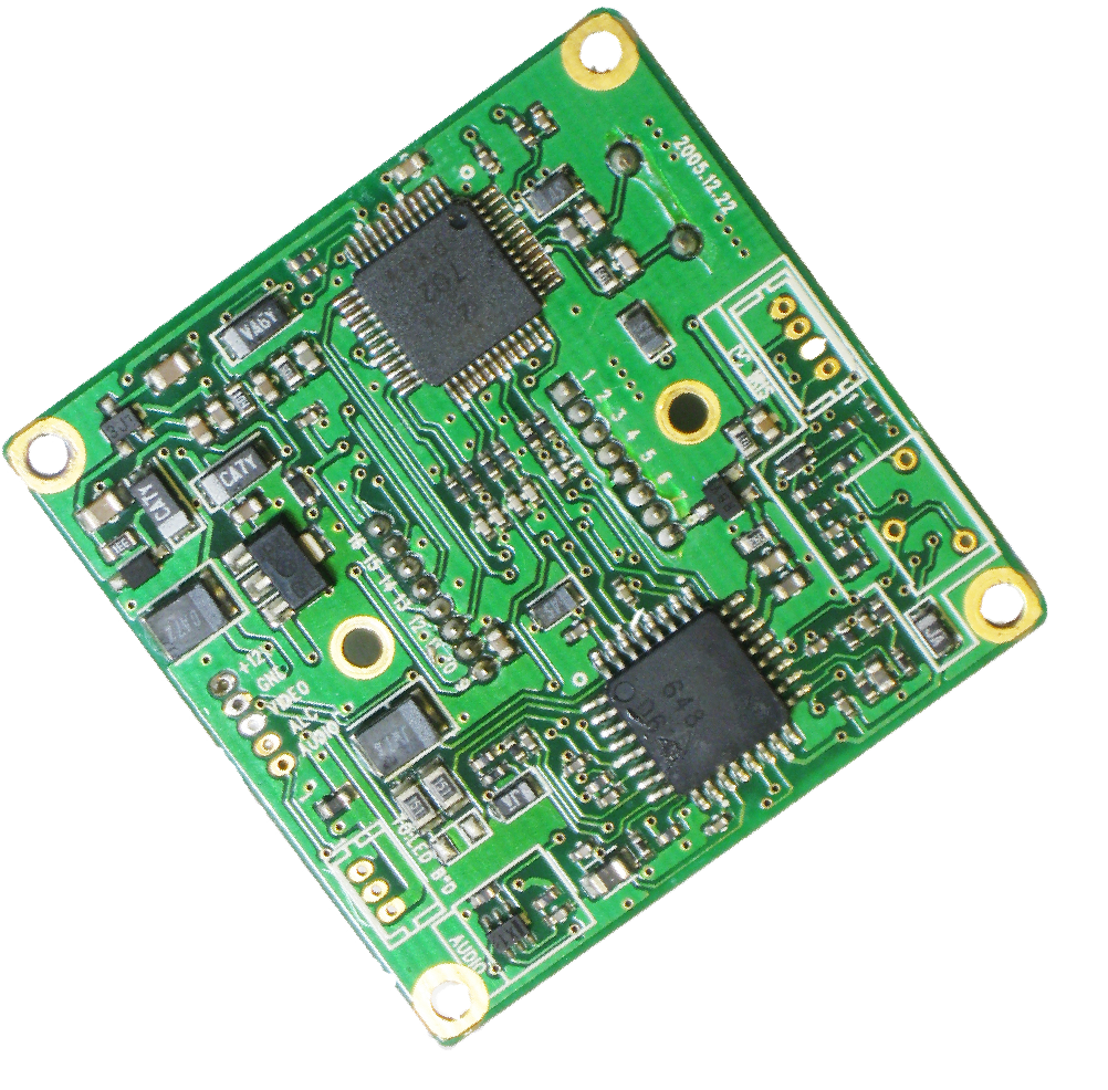
 PCB(Printed Circuit Board) is a conductive pattern formed on conductive material according to the engineers’ design, there solely traces/ holes/ layer on it, however with none components installed. Firstly, we should speak about the PCB and PCBA, what is the difference? Assembly) means bare PCB board assembled with components similar to resistors/ capacitors/ IC, to make the whole circuit board works as intended. After the PCB was designed by digital engineers, the files(Normally production files, called Gerber information, however not authentic design files schematic& PCB layout, to maintain the original design protected, and thus to guard the mental property) could be despatched to PCB factories for manufacturing. Meanwhile, after elements sourced, after which they are often installed on the PCB board, and last programming, testing… And finally a PCBA manufactured, that be ready for an electronic undertaking. But this is not actually an easy work, especially for a maker & startup, there’re many processes to create a working PCBA board… Makerfabs provides the turnkey PCBA service from PCB manufacturing, components sourcing, PCB board assembly, soldering, programming, testing to end shipping. With this one-stop and quick turn PCB assembly service, the digital designers don’t must undergo from these very detailed works equivalent to soldering the prototype board, and thus can focus on the electronics creating and PCBA designing works.
 The process by which the bare printed circuit boards, PCBs utilized in electronic merchandise is evey bit as necessary because the assembling with elements. PCB manufacture basics How to choose the right PCB producer The PCB manufacturing process is essential for anyone concerned in the electronics industry. Printed circuit boards, PCBs, are very broadly used as the premise for electronic circuits. Printed circuit boards are used to offer the mechanical foundation on which the circuit can be built. Accordingly nearly all circuits use printed circuit boards and they are designed and used in quantities of hundreds of thousands. Although PCBs kind the basis of virtually all electronic circuits at the moment, they are typically taken as a right. Nevertheless technology in this area of electronics is shifting forward. Track sizes are lowering, the numbers of layers within the boards is rising to accommodate for the elevated connectivity required, and the design guidelines are being improved to make sure that smaller SMT gadgets could be handled and the soldering processes used in production can be accommodated.
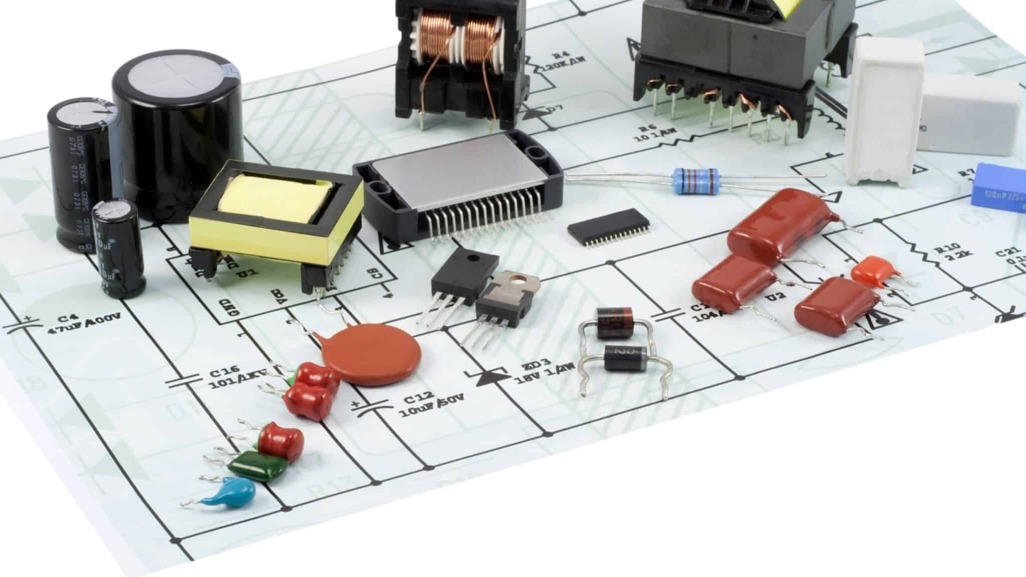
The PCB manufacturing course of may be achieved in a selection of how and there are a number of variants. Despite the many small variations, pcb assembly cost the primary stages in the PCB manufacturing process are the same. Printed circuit boards, PCBs, might be made from quite a lot of substances. The most widely used in a type of glass fibre based board known as FR4. This offers a reasonable degree of stability beneath temperature variation and is does not breakdown badly, whereas not being excessively costly. Other cheaper supplies can be found for the PCBs in low value business products. If you beloved this posting and you would like to obtain extra details about Pcb assembly Cost kindly stop by the website. For top performance radio frequency designs the place the dielectric fixed of the substrate is vital, and low ranges of loss are needed, then PTFE based printed circuit boards can be used, although they are far harder to work with. In order to make a PCB with tracks for the parts, copper clad board is first obtained. This consists of the substrate material, typically FR4, with copper cladding usually on both sides.
This copper cladding consists of a thin layer of copper sheet bonded to the board. This bonding is normally superb for FR4, however the very nature of PTFE makes this harder, and this provides problem to the processing of PTFE PCBs. With the naked PCB boards chosen and obtainable the next step is to create the required tracks on the board and take away the undesirable copper. The manufacture of the PCBs is often achieved utilizing a chemical etching course of. The most common form of etch used with PCBs is ferric chloride. In order to gain the proper sample of tracks, a photographic process is used. Typically the copper on the naked printed circuit boards is coated with a skinny layer of picture-resist. It is then exposed to light by a photographic movie or photograph-mask detailing the tracks required. In this manner the picture of the tracks is passed onto the picture-resist.